Cmos Inverter 3D / Create Contact And Metal M1 Cmos Processing Part 6 Vlsi Concepts / The device symbols are reported below.. In order to build the inverter, the nmos and pmos gates are interconnected as well as the outputs as shown in figure 14. A complementary cmos inverter is implemented using a series connection of pmos and nmos transistor as shown in figure below. Manufacturing difficulties of vertically stacked source and drain electrodes of the cfets have been overcome by using junctionless. This note describes several square wave oscillators that can be built using cmos logic elements. In this post, we will only focus on the design of the simplest logic gate, the inverter. we will try to understand the working of the cmos inverter.
Effect of transistor size on vtc. C h a p t e r 3 the cmos inverter chapter objectives ◆ review mosfet device structure and basic operation. The cmos inverter the cmos inverter includes 2 transistors. This note describes several square wave oscillators that can be built using cmos logic elements. Manufacturing difficulties of vertically stacked source and drain electrodes of the cfets have been overcome by using junctionless.
3d View Of Cmos Inverter Youtube from i.ytimg.com This note describes several square wave oscillators that can be built using cmos logic elements. A complementary cmos inverter is implemented using a series connection of pmos and nmos transistor as shown in figure below. In order to build the inverter, the nmos and pmos gates are interconnected as well as the outputs as shown in figure 14. More experience with the elvis ii, labview and the oscilloscope. As you can see from figure 1, a cmos circuit is composed of two mosfets. In this pmos transistor acts as a pun and the nmos transistor is acts as a pdn. They operate with very little power loss and at relatively high speed. Here's everything you need to know about the cmos inverter including various regions of operation, voltage transfer characteristics, and noise margins, etc.
As you can see from figure 1, a cmos circuit is composed of two mosfets.
Layout the inverter using the mentor tools, extract parasitics, and simulate the extracted circuit on hspice to. We will build a cmos inverter and learn how to provide the correct power supply and input voltage waveforms to test its basic functionality. As you can see from figure 1, a cmos circuit is composed of two mosfets. The device symbols are reported below. Posted tuesday, april 19, 2011. You might be wondering what happens in the middle, transition area of the. Switching characteristics and interconnect effects. Experiment with overlocking and underclocking a cmos circuit. Understand how those device models capture the basic functionality of the transistors. The cmos inverter collections found on the site are equipped with all the fascinating features such as intelligent cooling technology for faster and smart browse through the varied cmos inverter ranges at alibaba.com and buy the best of these products. In order to plot the dc transfer. Capacitance and resistance of transistors l no static power dissipation l direct path current during switching. Now, cmos oscillator circuits are.
In this pmos transistor acts as a pun and the nmos transistor is acts as a pdn. The pmos transistor is connected between the. The cmos inverter the cmos inverter includes 2 transistors. Voltage transfer characteristics of cmos inverter : A common issue for any cmos circuit is the existance of a parasitic thyristor resulting from the npnp structure that exists between any in this example, body ties and implanting the base of the trench, are deliberatly omitted, making this cmos inverter particularly vulnerable to thyristor action.
Functional Transformation In 3d Transient Cmos Logic Gates A Optical Download Scientific Diagram from www.researchgate.net Switching characteristics and interconnect effects. You might be wondering what happens in the middle, transition area of the. These circuits offer the following advantages Furthermore, the cmos inverter has good logic buffer. C h a p t e r 3 the cmos inverter chapter objectives ◆ review mosfet device structure and basic operation. Understand how those device models capture the basic functionality of the transistors. Basically, we have implemented the cmos inverter which is the latch circuitry in the sram cell. Voltage transfer characteristics of cmos inverter :
The cmos inverter the cmos inverter includes 2 transistors.
Now, cmos oscillator circuits are. As you can see from figure 1, a cmos circuit is composed of two mosfets. The cmos inverter the cmos inverter includes 2 transistors. Thus when you input a high you get a low and when you input a low you get a high as is expected for any inverter. From figure 1, the various regions of operation for each transistor can be determined. The device symbols are reported below. This note describes several square wave oscillators that can be built using cmos logic elements. ◆ analyze a static cmos. Make sure that you have equal rise and fall times. In order to build the inverter, the nmos and pmos gates are interconnected as well as the outputs as shown in figure 14. Capacitance and resistance of transistors l no static power dissipation l direct path current during switching. Cmos devices have a high input impedance, high gain, and high bandwidth. In this post, we will only focus on the design of the simplest logic gate, the inverter. we will try to understand the working of the cmos inverter.
More experience with the elvis ii, labview and the oscilloscope. The cmos inverter the cmos inverter includes 2 transistors. Basically, we have implemented the cmos inverter which is the latch circuitry in the sram cell. The pmos transistor is connected between the. In order to plot the dc transfer.
How Cmos Works Some Final Words About Cmos Hackaday from hackaday.com You might be wondering what happens in the middle, transition area of the. Voltage transfer characteristics of cmos inverter : ◆ analyze a static cmos. The cmos inverter collections found on the site are equipped with all the fascinating features such as intelligent cooling technology for faster and smart browse through the varied cmos inverter ranges at alibaba.com and buy the best of these products. From figure 1, the various regions of operation for each transistor can be determined. Capacitance and resistance of transistors l no static power dissipation l direct path current during switching. Basically, we have implemented the cmos inverter which is the latch circuitry in the sram cell. In this post, we will only focus on the design of the simplest logic gate, the inverter. we will try to understand the working of the cmos inverter.
Experiment with overlocking and underclocking a cmos circuit.
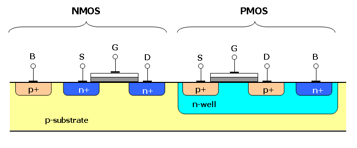
Make sure that you have equal rise and fall times. Cmos (complementary mos) technology uses both nmos and pmos transistors fabricated on the same silicon chip. The cmos inverter collections found on the site are equipped with all the fascinating features such as intelligent cooling technology for faster and smart browse through the varied cmos inverter ranges at alibaba.com and buy the best of these products. • design a static cmos inverter with 0.4pf load capacitance. Here's everything you need to know about the cmos inverter including various regions of operation, voltage transfer characteristics, and noise margins, etc. The device symbols are reported below. Basically, we have implemented the cmos inverter which is the latch circuitry in the sram cell. These circuits offer the following advantages C h a p t e r 3 the cmos inverter chapter objectives ◆ review mosfet device structure and basic operation. ◆ analyze a static cmos. More experience with the elvis ii, labview and the oscilloscope. Now, cmos oscillator circuits are. Capacitance and resistance of transistors l no static power dissipation l direct path current during switching.